Because the physical traces on a circuit board can cause signal delays that exceed the timing tolerances of high-speed memory, DDR3 and DDR4 systems must undergo a calibration process at every boot to align data with the system clock. This process, documented in the LiteDRAM project, compensates for the fact that different memory chips on the same rank receive the clock signal at slightly different times due to their physical distance from the controller.
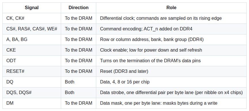
This table provides specific technical parameters related to the memory interface configurations discussed in the article.
The Challenge of Fly-By Topology
DDR3 and DDR4 memory interfaces utilize a fly-by topology for the clock, command, and address pins. In this layout, the signals pass by each memory chip in turn before reaching a termination point, which keeps the heavily loaded signals clean at high speeds.
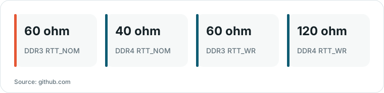
Chart drawn by HN Digest from figures reported by github.com; values are shown as written in the source.
The trade-off is that each chip receives the clock a little later than the previous one. Because the data lanes are point-to-point, their delays do not follow the clock, creating a skew between the first and last chip that can exceed a single clock period.
“With fly-by routing the skew between the first and the last chip can exceed a clock period, so each lane needs its own DQS delay.”
— litedram/doc/manual/03_dram_interface.md at master · enjoy-digital/litedram
Write Leveling and Latency Calibration
To correct for fly-by skews, the controller performs 'write leveling.' It puts the DRAM into a special mode and sends DQS pulses, measuring the delay until the DRAM returns a specific bit transition. The controller then adjusts the output delays for each lane until DQS is perfectly aligned with the clock (CK) at that specific chip.
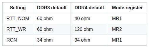
This table supports the discussion of specific hardware configurations and signal behaviors in high-speed memory systems.
Beyond alignment, the system must also calibrate write latency and DQ-DQS training. This ensures that a lane is not one whole clock early or late, and that the data (DQ) is centered against the strobe (DQS) during the write operation.
Read Leveling and the Data Eye
On the read side, the controller does not know exactly when data will arrive because board and I/O delays differ per lane. Read leveling finds two settings for each lane: a coarse 'bitslip' to align the word to the correct clock cycle, and a fine input delay to find the 'data eye.'
The data eye is the window where the first word of a read arrives at the correct bit position. A wide window indicates a robust interface, while a narrow window suggests signal integrity or clocking issues. On some hardware, such as the Lattice and Gowin PHYs, the system must also use a 'burst detect' to identify when the DRAM is actually sending data.
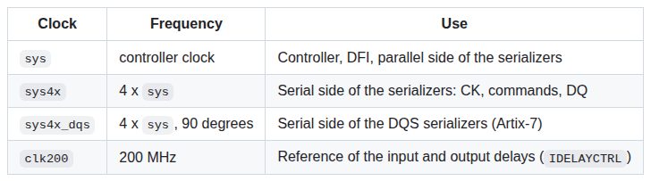
This visual provides additional context for the read leveling and data eye measurements described in the text.
Hardware Constraints and Trade-offs
Not all hardware supports the same level of calibration. For example, the Artix-7 FPGA lacks the output delays required for standard write leveling on all lanes, forcing the system to use a static DQS phase or a CK phase shift mode.
Furthermore, while the UltraScale+ PHY can set the FPGA read VREF (reference voltage) in steps, the LiteDRAM BIOS currently leaves this at a build-time value unless manually adjusted by software. These limitations highlight how physical hardware constraints directly dictate the supported memory configurations.