AMD's Zen 6 architecture achieves a generational uplift over Zen 5 by doubling the number of VNNI units to four per cycle and allowing a single thread to utilize both of the core's decode clusters. These changes, combined with a new 'Zen 6c' variant, signal a shift in AMD's strategy toward specializing core designs for different workload behaviors rather than simply scaling the same core to different densities.
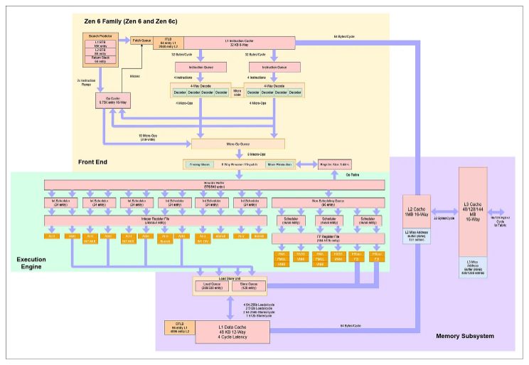
This figure provides a high-level overview of the Zen 6 architecture and its core design philosophy.
Frontend and Branch Prediction Improvements
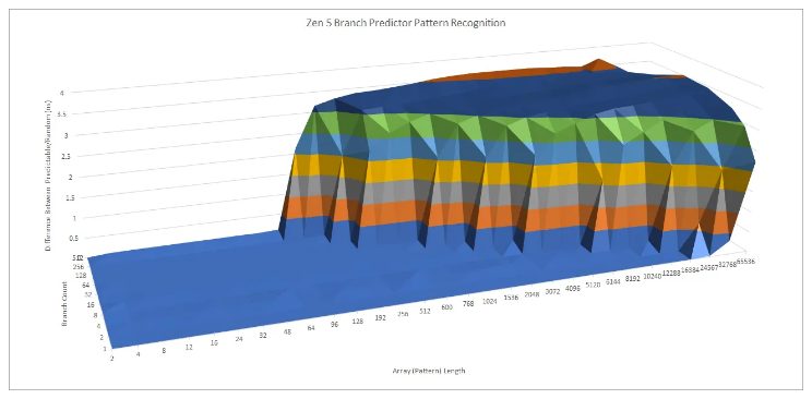
Zen 6 builds on the direction predictor of Zen 5 but improves the core's ability to recover from mispredictions. While Zen 5 took roughly 3.5 to 4 ns to recover from a wrong guess, Zen 6 reduces this penalty to 3 to 3.5 ns.
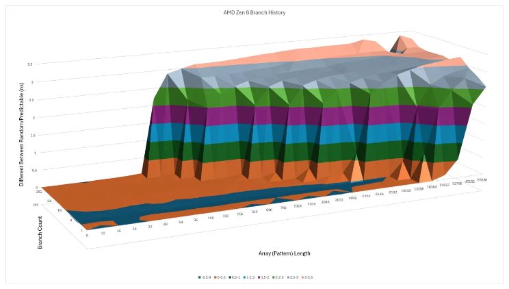
The chart illustrates the specific improvement in branch prediction recovery times mentioned in the text.
A significant architectural shift occurs in the instruction fetch stage. Unlike Zen 5, where a single thread could only effectively use one decode cluster, Zen 6 allows a single thread to utilize both clusters simultaneously, increasing potential instruction throughput.
This image supports the description of the architectural shift in the instruction fetch stage.
“The differences suggest that AMD is specializing the two designs. Zen 6 appears tuned for high frequency, while Zen 6c has more capacity to tolerate comparatively high memory latency.”
— AMD’s Zen 6 Family: Feeding the Beast
Execution Engine and Vector Throughput
On the integer side, Zen 6 returns to a Zen 4-style NOP pairing behavior, allowing the core to retire up to 16 NOPs per cycle. It also improves theoretical peak throughput for simple 64-bit adds, reaching 5.96 per cycle compared to Zen 5's 5.25.
AMD reduced the number of integer multiply units from three to two, citing that the third unit did not justify its area cost. Conversely, the vector side sees a major boost in VNNI units, which are critical for AI inference and video codecs, doubling from two to four units per cycle.
The Zen 6 vs. Zen 6c Architectural Split
For the first time, the 'Classic' and 'Dense' cores differ within the out-of-order engine. Zen 6 is tuned for high frequency, while Zen 6c is designed to absorb latency by increasing the capacity of internal structures.
Zen 6c features a larger reorder buffer (640 vs. 576 entries), a larger integer register file (352 vs. 288), and a larger load queue (330 vs. 280). These changes allow Zen 6c to keep more work 'in flight' to mask the effects of slow memory access.
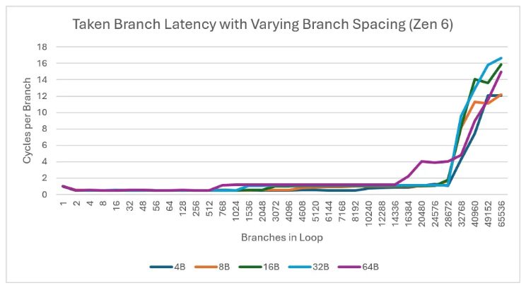
This figure visually represents the capacity differences that allow Zen 6c to mask memory latency.
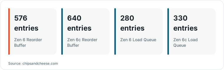
Chart drawn by HN Digest from figures reported by chipsandcheese.com; values are shown as written in the source.
Performance Trade-offs and Memory Scaling
The EPYC 9686F (Zen 6) outperforms the 9996 (Zen 6c) in raw integer and floating-point rates because it can maintain higher clock speeds. However, the 9996's 128 MB L3 cache helps it maintain lower memory-stall shares in heavy workloads like 'fotonik3d' and 'lbm'.
L3 latency has increased across the family, reaching 55 cycles on Zen 6 and 66 cycles on Zen 6c. While the higher clock on Zen 6 hides much of this increase, the larger cache on Zen 6c serves as a primary mechanism to reduce the need to access main memory.
What Hacker News readers are saying
- Technical note: One commenter noted that the increased out-of-order structures in the Zen 6c variant appear to be a strategic move to absorb memory latency as workloads become more memory-heavy. comment ↗
- Technical note: A reader expressed curiosity regarding the reduction in integer multipliers and PDEP/PEXT throughput, questioning whether these operations share the same circuitry or represent independent hardware cuts. comment ↗
- Skeptical: Several commenters discussed the limitations of memory bandwidth, with one observer noting that many applications are IO-bound rather than compute-bound, while another argued that reducing memory latency is more critical than increasing bandwidth. comment ↗
- Technical note: One commenter raised an open question about the architectural management of 32 cores on a single CCD, specifically asking if there will be smaller logical units between the CCD and the individual cores. comment ↗
Summarized opinions from the Hacker News thread, not verified facts. Read the full discussion ↗