By exploiting a voltage fault injection (VFI) vulnerability, a researcher successfully converted a CMP 170HX 8GB mining card into a high-performance configuration that performs approximately 1.18x faster than a retail NVIDIA A100. This was achieved by bypassing the hardware fuses that NVIDIA uses to 'floorsweep' or disable specific components on the GA100 die to segment products based on manufacturing yield and market demand.
The Mechanism of Hardware Segmentation
NVIDIA utilizes a fuse controller on the GA100 die to manage product segmentation and security. This controller contains over 16,000 eFuses that provide 'option words' to the rest of the die, determining which features are active and which hardware blocks are powered down.
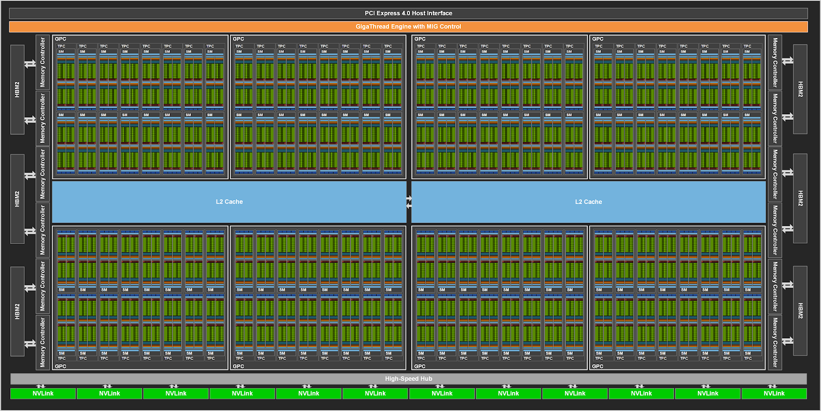
This diagram illustrates the internal layout of the GA100 die, providing context for how the fuse controller manages different hardware blocks.
A critical mechanism in this process is 'floorsweeping,' where specific fuse values trigger signals that render die elements unreachable. For example, the OPT_FBP_DISABLE fuse can mask specific Framebuffer Partitions (FBP), effectively reducing the available memory or compute power of the chip.
“NVIDIA’s design allows one to relax restrictions by blowing more fuses!”
— Using voltage glitching to unleash the A100 in my mining card
Bypassing Fuses via Voltage Fault Injection
The researcher identified a vulnerability where voltage fault injection can be used to defeat the fuse controller's safeguards. This allows an operator to program 'Fuseless fuses' (FF), which are structured as a JTAG-chain-like script to define the die's functional options.
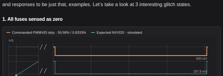
This figure represents the initial state of the fuses before the researcher successfully injected faults to bypass security.
By injecting voltage faults, the researcher was able to write new FF rows that set the '_DISABLE' words to zero. This effectively 'unblocks' the floorswept components, allowing the hardware to utilize its full potential regardless of its original intended SKU.
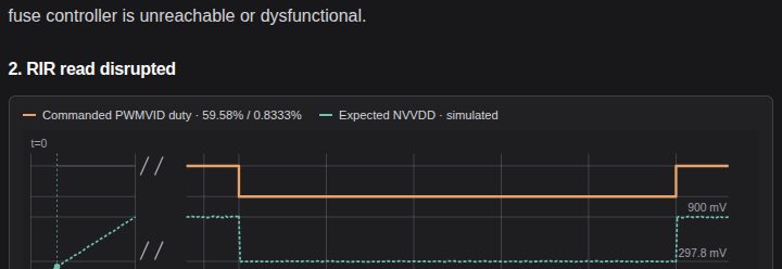
This image depicts the specific mechanism of the voltage fault injection used to defeat the fuse controller's safeguards.
Performance Gains and Limitations
The primary result of this unlock is a significant increase in compute capacity. Because the retail A100 is limited to 108 SMs to ensure high manufacturing yields, the unlocked card—which enables 120 to 126 SMs depending on the specific die lot—surpasses the retail unit's performance.
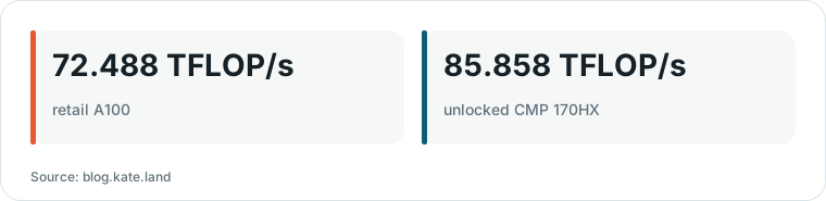
Chart drawn by HN Digest from figures reported by blog.kate.land; values are shown as written in the source.
While the method can unlock high-end features like NVLink and PCIe Gen4, certain functionalities like NVJPG, NVDEC, and MIG remain untested in this specific configuration. Furthermore, the success of the unlock is dependent on the specific die lot and the number of functional SMs available on the original chip.