In 1965, Signetics introduced the 600 series, the first integrated circuit family offered in a solid, plastic, dual in-line package (DIP). This shift from metal cans to plastic allowed for easier manual and automated assembly, helping to popularize the DIP format that remains a standard in electronics today. A recent reverse-engineering of the ST680A chip—a quad NAND gate from this era—provides a rare look at the transition from Resistor-Transistor Logic (RTL) to the diode-based architectures that preceded modern Transistor-Transistor Logic (TTL).
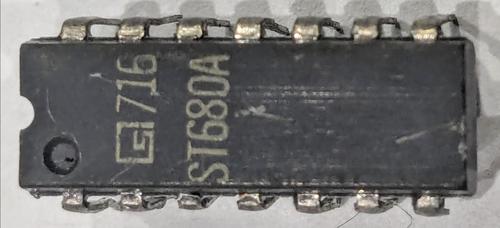
This image shows the physical package of the ST680A chip, which was part of the first integrated circuit family offered in a plastic DIP.
Microscopic Architecture of DTL
The ST680A die is constructed from bipolar NPN transistors, which differ significantly from the MOS transistors used in modern integrated circuits. In these NPN transistors, the current from the collector to the emitter is controlled by the base current, with the collector appearing as a large region of N-type silicon (reddish) and the base as a thin layer of P-type silicon (green).
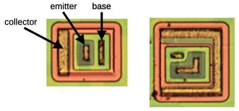
The article describes the construction of the die from bipolar NPN transistors, where the collector appears as a large reddish region.
To facilitate logic operations, the chip incorporates 16 resistors made from long, thin strips of doped silicon. These resistors use a serpentine layout to maximize length within a small area. They are housed in 'tubs' of N-type silicon, which isolate the resistors from one another by preventing current flow between the P-type and N-type regions.
“This approach used a custom metal layer on top of fixed silicon, providing custom circuits without the cost of a full mask set.”
— Reverse engineering a vintage diode-transistor logic chip
The Mechanism of the DTL NAND Gate
Diode-Transistor Logic (DTL) was designed to provide better performance than Resistor-Transistor Logic (RTL) by replacing resistors on the inputs with diodes. In a DTL NAND gate, if both inputs are high, current flows through the first transistor's base, turning it on and amplifying the current to the second transistor. This pulls the output pin low.
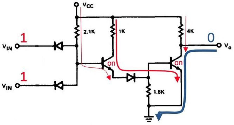
The schematic explains the mechanism of the DTL NAND gate, showing how current flows through the transistors to pull the output low.
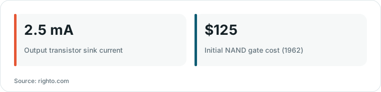
Chart drawn by HN Digest from figures reported by righto.com; values are shown as written in the source.
If one input is pulled low, the current flows through a diode instead of the transistor, keeping the second transistor off. A third resistor then pulls the output high. While effective, this design has a notable limitation: the output resistor continues to 'try' to pull the output high even when the output is low, resulting in wasted power and a relatively weak high signal.
Semi-Custom Manufacturing and VariFEBS
A key finding in the reverse engineering of the ST680A is the presence of 'extra' diodes that seemed to belong to unused inputs. This was explained by Signetics' 'variFEBS' approach, where the company used the same silicon layout for at least three different chips—the 680A, 670A, and 616A—by simply applying different metal layers to create different functionalities.
This strategy saved significant costs by avoiding the need for a complete set of new optical masks for every chip variation. For example, the 616A dual-NAND chip used the 'extra' diodes found on the 680A die to support its higher input count. This method allowed Signetics to offer semi-custom circuits to customers without the overhead of full-scale production for every unique design.
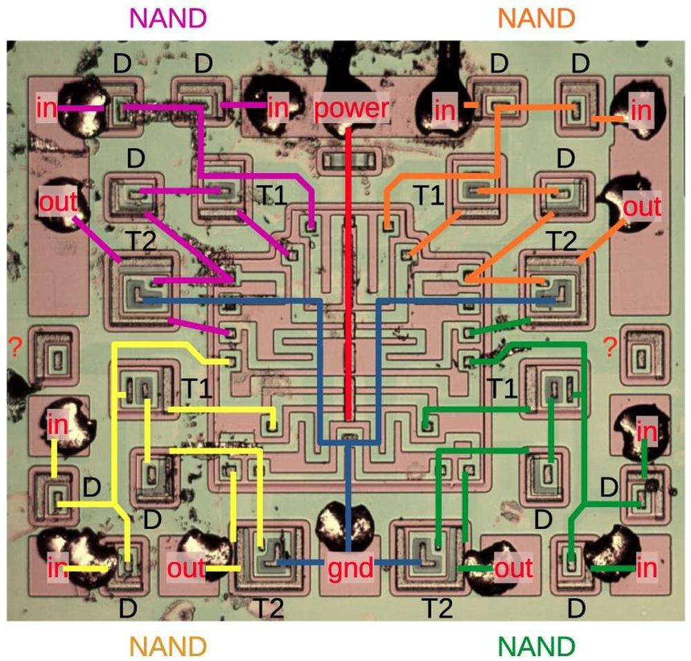
This visual illustrates the 'variFEBS' approach where different metal layers were applied to the same silicon layout to create different chips.