Infineon Technologies has successfully processed 300-millimeter silicon carbide (SiC) wafers into functional power devices at its Villach, Austria facility. This marks the first time such a milestone has been achieved in a full-scale semiconductor fab environment, utilizing existing silicon manufacturing equipment to scale production for the next generation of power electronics.
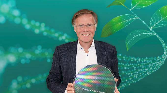
This photo depicts the specific milestone of processing 300mm SiC wafers into functional devices mentioned in the introduction.
Scaling Manufacturing Efficiency
The transition from 200mm to 300mm wafers represents a significant leap in manufacturing throughput. Because of the larger diameter, the 300mm format provides 2.3 times more chips per wafer, which is critical for meeting the rising demand for power semiconductors.
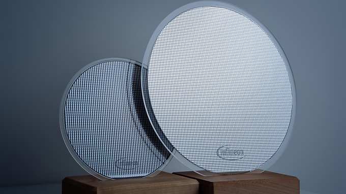
This image illustrates the physical size difference between the standard 200mm wafers and the new 300mm format discussed in the scaling section.
By utilizing existing silicon (Si) manufacturing equipment to process these wafers, Infineon has demonstrated that the technology is ready to move from laboratory research into a full-scale industrial manufacturing environment.
“Chip production on 300 mm wafers is technologically more advanced and significantly more efficient than 200 mm wafers, since the larger wafer diameter offers 2.3 times more chips per wafer.”
— Infineon marks innovation milestone with world’s first | Infineon Technologies
Material Advantages and Applications
Silicon carbide (SiC) is a key wide-bandgap material used for highly efficient power conversion. Its unique properties allow for lower power loss and higher power density, especially when operating at high voltages and temperatures.
These characteristics make SiC vital for traction inverters, on-board chargers, and large-scale energy storage. Additionally, the material is increasingly important in AI data centers for solid-state transformers and power supply units.
Technological Innovations in Wafer Processing
To support the 300mm scale, Infineon also successfully tested 'Cold Split' technology at its Dresden, Germany site. This method separates wafers from a SiC boule with less material loss and faster processing times than traditional wire sawing.
By reducing capital expenditure and material waste, Cold Split helps ensure a more cost-effective and secure supply base for customers in the automotive and industrial sectors.
Future Roadmap and Limitations
While this milestone establishes the feasibility of 300mm SiC, Infineon will continue to execute its existing 200mm manufacturing roadmap while planning the ramp timing for the new technology in collaboration with partners.
The source material does not currently specify the exact production costs, yield rates, or the specific timeline for when these 300mm SiC products will be commercially available to the public.
What Hacker News readers are saying
- Alternative: One commenter suggested that restarting DRAM production in Europe would be a more economically viable opportunity than the current focus. comment ↗
- Experience: Another reader argued that while the news might not seem flashy, power semiconductors are critical for national security and industrial infrastructure like trucks and cars. comment ↗
- Skeptical: A commenter pointed out that memory packaging is highly complex and that Europe currently lacks the major players and capital investment found in Asia and the US. comment ↗
Summarized opinions from the Hacker News thread, not verified facts. Read the full discussion ↗