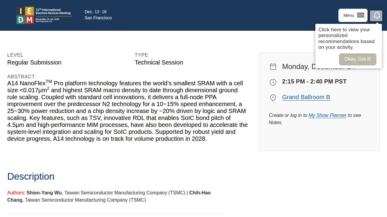
Taiwan Semiconductor Manufacturing Company (TSMC) has revealed the specifications for its A14 NanoFlex Pro platform, a next-generation manufacturing node designed for high-performance computing (HPC), AI, and mobile System-on-Chip (SoC) applications. The A14 node serves as the successor to the N2 technology, incorporating 2nd generation nano-sheet architecture to drive improvements in power, performance, and area (PPA). TSMC expects the technology to be ready for volume production by 2028.
The platform's core advancement lies in its ability to achieve the world’s smallest SRAM with a cell size of less than 0.017μm. By utilizing dimensional ground rule scaling and standard cell innovations, the A14 node aims to deliver a 10-15% speed enhancement and a 25-30% reduction in power consumption compared to the N2 node. Additionally, the technology provides a roughly 20% increase in chip density. To support system-level integration, particularly for System-on-Integrated-Chips (SoIC), the platform includes Through-Silicon Via (TSV) technology, high-performance Metal-Insulator-Metal (MiM) processes, and an innovative Redistribution Layer (RDL) that enables a 4.5μm bond pitch.
While the 20% density increase is a significant technical milestone, it reflects a decelerating trend in semiconductor scaling. Commenters on Hacker News noted that previous generations, such as the jump from N10 to N3, saw density gains of 60-80%, suggesting that the physical limits of silicon are becoming harder to overcome. Despite these diminishing returns, some observers pointed out that even modest gains in SRAM density can be critical, as SRAM often dominates the surface area of a chip. However, the source material does not clarify whether the increased manufacturing costs for such advanced sub-atomic precision will outweigh the 20% density gains, leaving the ultimate cost-per-transistor impact for the A14 node an open question.