The Raspberry Pi RP2350 microcontroller introduced several security features, including a Secure Boot implementation and a 'Redundancy Co-Processor' (RCP) designed to mitigate fault injection and return-oriented programming attacks. To test these defenses, a hacking challenge was launched during DEFCON 2024, requiring participants to recover secret data from a locked Pico 2 board. While many participants found that the RP2350's integrated glitch detectors effectively blocked standard voltage fault injection attacks, researcher Kévin Courdesses (courk) successfully bypassed the security by employing laser fault injection (LFI).
Laser fault injection works by directing a focused laser beam at the silicon die of a chip. The photoelectric effect allows the light to induce temporary malfunctions in transistors, which can be timed to skip instructions or corrupt register values. Because the RP2350's glitch detectors are designed to sense voltage or electromagnetic fluctuations, Courdesses targeted the die from the backside to bypass these sensors. This required a complex preparation process: desoldering the RP2350, mechanically grinding away the metallic ground pad using a low-cost engraving tool, and then using conductive epoxy to restore a sufficient ground connection to the internal circuitry. This method allowed the laser to interact with the die without triggering the chip's internal security resets.
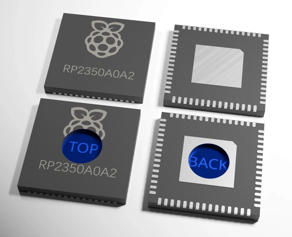
This image illustrates the physical structure of an integrated circuit, which is necessary for understanding how backside laser attacks bypass internal sensors.
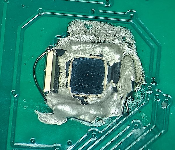
This photo shows the specific preparation step where conductive epoxy is used to maintain electrical integrity while allowing laser access.
To execute the attack, Courdesses developed a custom 'Laser Fault Injection Platform' using off-the-shelf components and 3D-printed parts. The system includes a main carrier board, an I/O board, and a laser driver board controlled by an FPGA to synchronize the laser pulses with the chip's boot sequence. By targeting specific instructions in the Boot ROM that are not hardened with redundant checks or random delays, the researcher was able to induce a single-instruction 'skip' or a register value corruption. This successfully bypassed the Secure Boot mechanism, allowing access to the protected OTP (One-Time Programmable) memory area where the secret data was stored. While the platform is budget-oriented, it demonstrates that high-precision hardware attacks can be achieved outside of industrial labs using accessible tools.
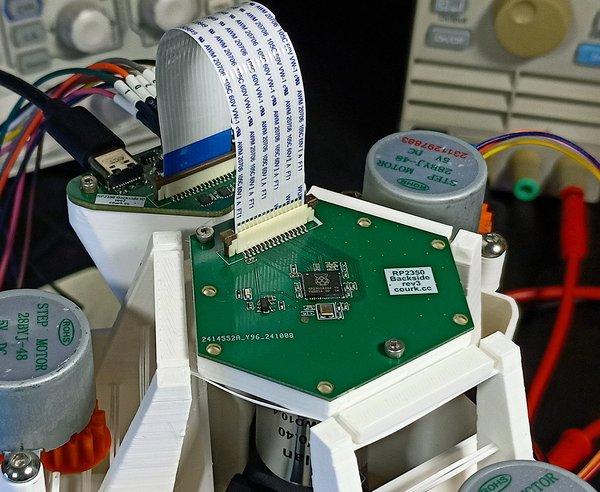
This image depicts the hardware components of the custom platform described in the third paragraph of the article.
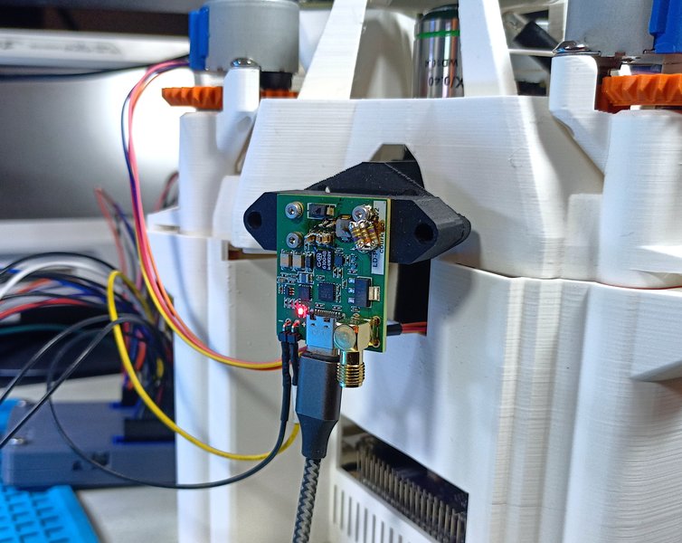
This visual complements the description of the platform's hardware, specifically the laser driver board mentioned in the final paragraph.